
74HCT244 SMD IC SOIC 20 Octal Buffer Line Driver Non Inverting Tri State TTL Compatible High Speed CMOS Logic IC (74HCT244 IC)
₹ 17.70 (Inclusive of 18.00% GST)
Base Price: ₹ 15.00 | GST (18.00%): ₹ 2.70
In Stock
Secure payments powered by Razorpay


Pune Store Pickup – Free
Order before 5 PM • Ready in approx. 2 hours
Collect upto 7:30 PM (Mon – Sat)
Collect upto 7:30 PM (Mon – Sat)
Dispatch from Pune
Orders before 3 PM: Same day dispatch
Orders after 3 PM: Next day dispatch
(No dispatch on Sunday)
Orders after 3 PM: Next day dispatch
(No dispatch on Sunday)
Buying in bulk?
Secure Payments100% safe and trusted
GST InvoiceWith every order
Wide Product RangeComponents, modules, tools and more
Product SupportQuick assistance via email
74HCT244 SMD IC SOIC 20 Octal Buffer Line Driver Non Inverting Tri State TTL Compatible High Speed CMOS Logic IC (74HCT244 IC)
The 74HCT244 is a high speed CMOS octal buffer line driver with TTL compatible input levels. It is designed for signal buffering and data driving in digital systems with non inverting outputs and tri state control for bus interfacing.
Key Features -
- Octal non inverting buffer line driver
- Tri state outputs for bus control
- TTL compatible input levels (HCT series)
- Two enable inputs for independent control
- High speed CMOS logic performance
- High current drive capability
- Low power consumption
- SMD SOIC 20 package
Specifications -
- IC type - octal buffer line driver non inverting
- Logic family - HCT CMOS TTL compatible
- Package type - SOIC 20 SMD
- Supply voltage - approx 4.5V to 5.5V
- Input type - TTL compatible
- Output type - tri state non inverting
- Propagation delay - approx 10ns to 15ns typical
- Output current - approx 6mA to 8mA
- Operating temperature - approx -40 to 85 degree C
Applications -
- Data buffering and signal isolation
- Bus driver circuits
- Microcontroller and memory interfacing
- Digital communication systems
- Industrial control electronics
- Embedded system design
Pinout Configuration -
- A1 to A8 - input lines
- Y1 to Y8 - output lines
- G1 G2 - enable inputs active low
- Vcc - power supply
- GND - ground
Related Products
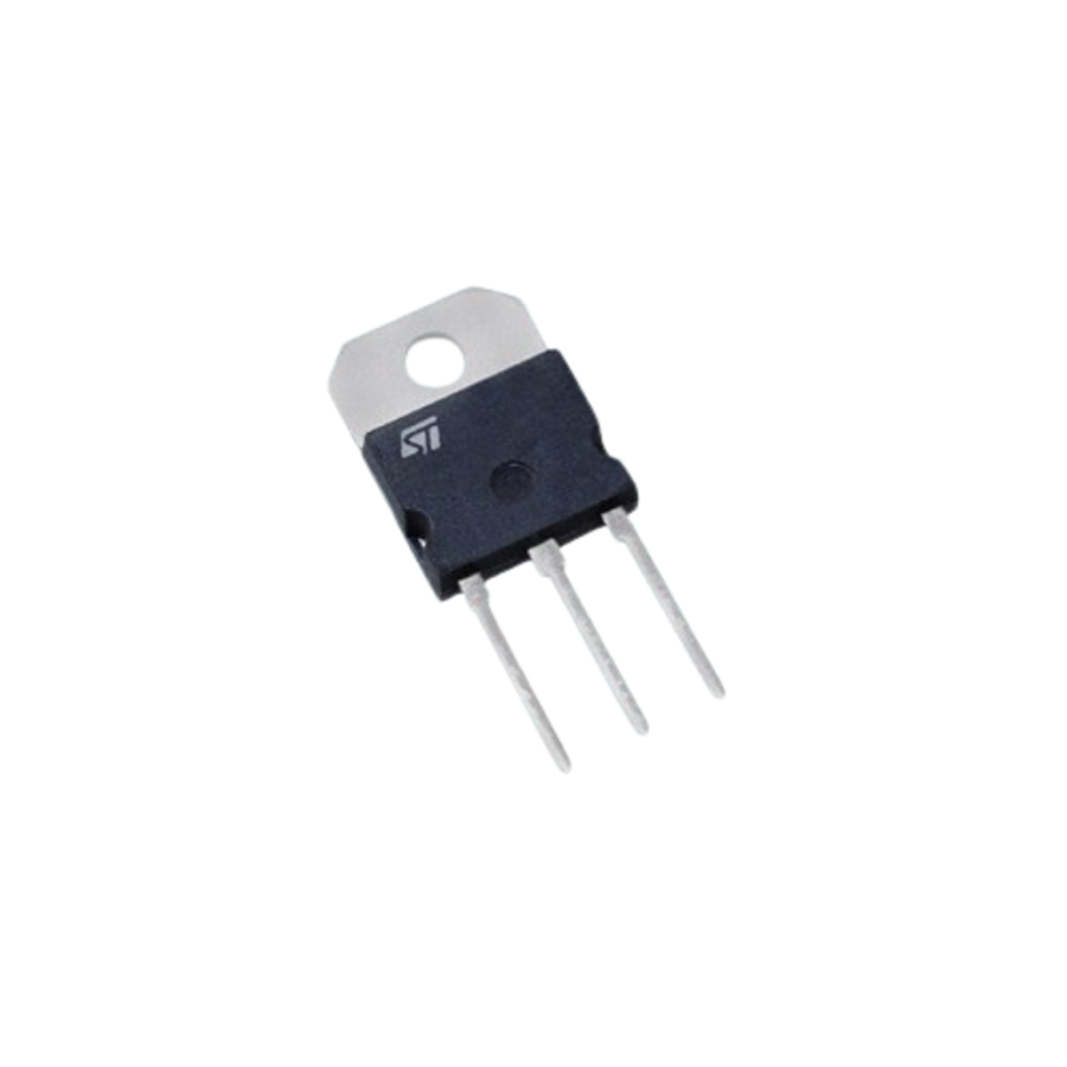 BDW83C NPN Darlington Power Transistor (15A, 150W, TO 3P, 1 Qty)
TRD-74
₹ 53.10 (Incl. GST)
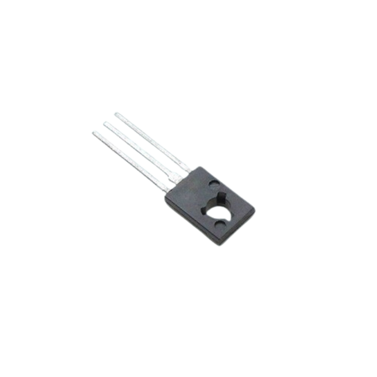 BD681 NPN Darlington Power Transistor (100V, 4A, TO 126, 1 Qty)
TRD-68
₹ 17.70 (Incl. GST)
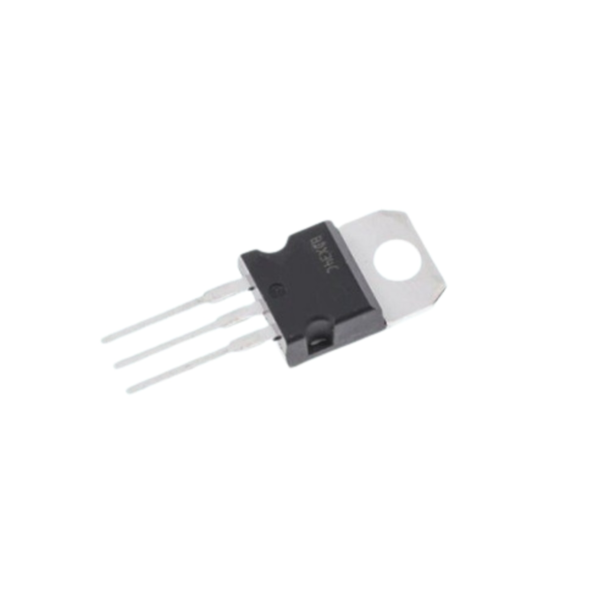 BDX34C PNP Darlington Power Transistor (100V, 10A, TO 220, 1 Qty)
TRD-69
₹ 53.10 (Incl. GST)
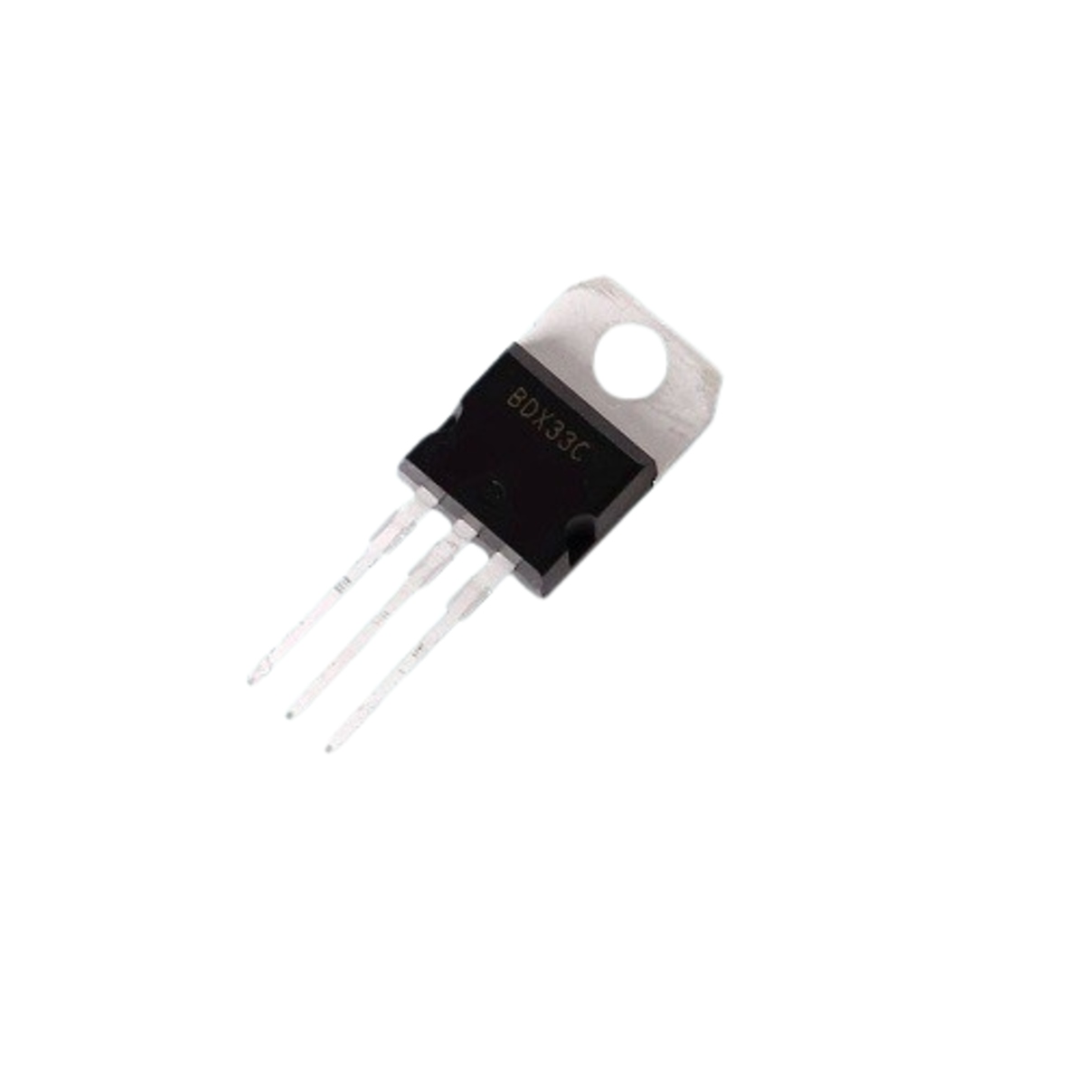 BDX33C NPN Darlington Power Transistor (100V, 10A, TO 220, 1 Qty)
TRD-70
₹ 23.60 (Incl. GST)
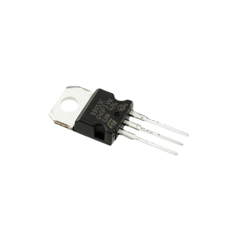 BDX53C NPN Darlington Power Transistor (100V, 8A, 60W, TO 220, 1 Qty)
TRD-71
₹ 23.60 (Incl. GST)
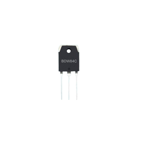 BDW84C Darlington Power PNP Transistor TO-3P (BDW84C Power Transistor)
TRD-72
₹ 53.10 (Incl. GST)
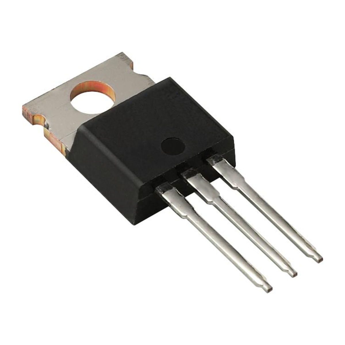 BDX34B PNP Darlington Power Transistor (80V, 10A, 70W, TO 220, 1 Qty)
TRD-73
₹ 53.10 (Incl. GST)
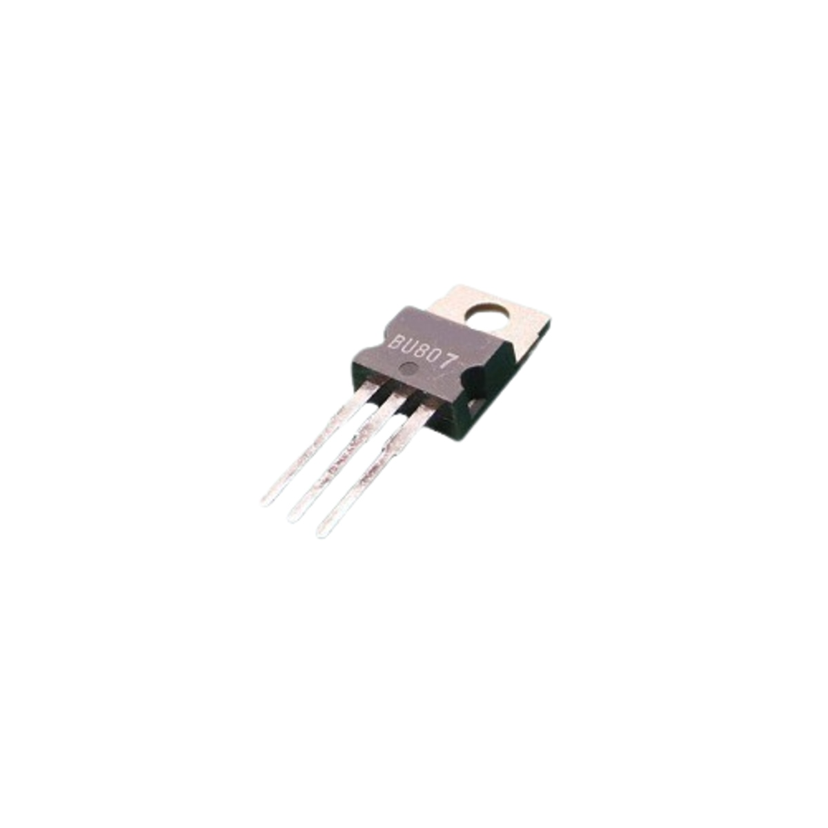 BU807 NPN Darlington Power Transistor (TO 220, 1 Qty)
TRD-77
₹ 27.10 (Incl. GST)
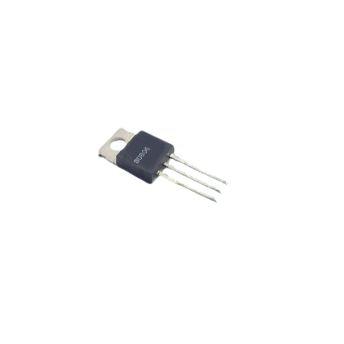 BU806 Multicomp Pro NPN Darlington Power Transistor (200V, 8A, 60W, TO 220, 1 Qty)
TRD-80
₹ 35.40 (Incl. GST)
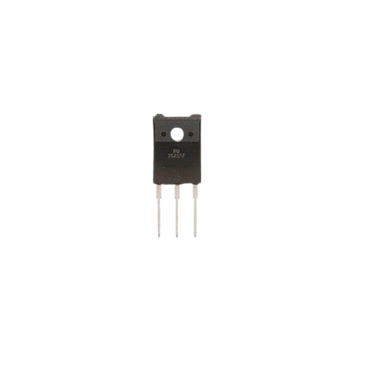 BU2508AF Silicon NPN Power Transistor (1500V, 8A, 80W, TO 247, 1 Qty)
TRD-79
₹ 118.00 (Incl. GST)