AD1674JNZ 12-Bit Analog-to-Digital Converter DIP-28 (AD1674JNZ IC)
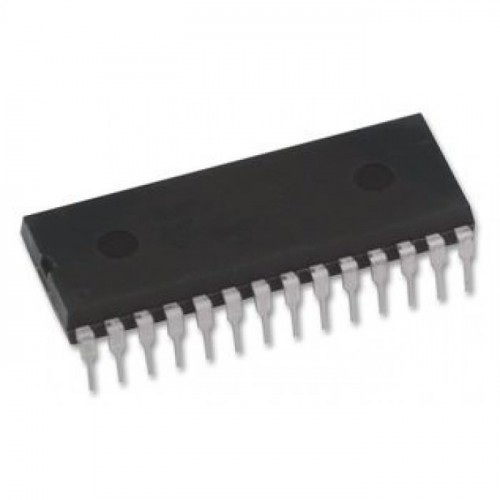
The AD1674JNZ is a high-performance, complete 12-bit Analog-to-Digital Converter (ADC) from Analog Devices. Housed in a standard 28-pin DIP package, it is a pin-compatible upgrade to the industry-standard AD674A and AD774B. It features an integrated internal reference, a clock, and a microprocessor interface with three-state output buffers. The device utilizes a successive-approximation architecture to achieve a conversion rate of 100 kSPS (10 microseconds).
This IC is a professional-grade component frequently used in industrial control systems, high-speed data acquisition, and medical instrumentation. In the Indian market, it is a preferred choice for legacy equipment maintenance and new designs requiring a reliable, high-resolution through-hole ADC that can handle various input voltage ranges (0V to +10V, 0V to +20V, +/-5V, and +/-10V) with minimal external circuitry.
Key Features
- 100 kSPS Throughput: Provides fast 10-microsecond maximum conversion time.
- Complete ADC: Includes an internal 10V buried Zener reference and a factory-trimmed clock.
- Microprocessor Compatible: Features a standard interface with three-state buffers for easy bus connection.
- Flexible Input Ranges: User-configurable for unipolar or bipolar inputs up to +/-10V.
- Low Power Consumption: Typical power dissipation of only 385mW.
- High Precision: Guaranteed no missing codes over the full operating temperature range.
- Pin Compatibility: Drop-in replacement for AD674A, AD774B, and AD574A (with faster timing).
Specifications
- IC Type: Successive Approximation ADC
- Resolution: 12-Bit
- Conversion Time: 10 us (Max)
- Sampling Rate: 100 kSPS
- Supply Voltage: +5V and +/-12V to +/-15V
- Reference Voltage: Internal 10V (Can also use external)
- Interface: Parallel (8-bit or 12-bit)
- Package Type: PDIP-28
- Mounting Type: Through-Hole
- Operating Temperature: 0 to 70 degrees Celsius
Interfaces
- Pin 1 (VCC): Digital +5V Supply
- Pin 2 (12/8): Data Mode Select (12-bit or 8-bit output)
- Pin 3 (CS/): Chip Select (Active Low)
- Pin 4 (A0): Byte Address/Short Cycle Control
- Pin 5 (R/C/): Read/Convert Control
- Pin 6 (CE): Chip Enable
- Pin 7 (VEE): Negative Supply (-12V to -15V)
- Pin 8 (REF OUT): +10V Reference Output
- Pin 9 (AGND): Analog Ground
- Pin 10 (REF IN): Reference Input
- Pin 11 (VLOGIC): Logic Supply (+5V)
- Pin 12 (BIP OFF): Bipolar Offset Adjustment
- Pin 13 (10V IN): 10V Span Input
- Pin 14 (20V IN): 20V Span Input
- Pin 15-22, 24-27 (DB0-DB11): Digital Data Outputs
- Pin 23 (STS): Status (High during conversion)
- Pin 28 (VCC): Positive Supply (+12V to +15V)