
CD4093 SOIC-14 Quad 2-Input NAND Schmitt Trigger IC (CD4093)
₹ 17.70 (Inclusive of 18.00% GST)
Base Price: ₹ 15.00 | GST (18.00%): ₹ 2.70
In Stock
Secure payments powered by Razorpay


Pune Store Pickup – Free
Order before 5 PM • Ready in approx. 2 hours
Collect upto 7:30 PM (Mon – Sat)
Collect upto 7:30 PM (Mon – Sat)
Dispatch from Pune
Orders before 3 PM: Same day dispatch
Orders after 3 PM: Next day dispatch
(No dispatch on Sunday)
Orders after 3 PM: Next day dispatch
(No dispatch on Sunday)
Buying in bulk?
Secure Payments100% safe and trusted
GST InvoiceWith every order
Wide Product RangeComponents, modules, tools and more
Product SupportQuick assistance via email
CD4093 SOIC-14 Quad 2-Input NAND Schmitt Trigger IC (CD4093)
The CD4093 is a CMOS Quad 2-Input NAND Schmitt Trigger IC designed for digital logic processing, waveform shaping, noise filtering, and oscillator applications. It contains four independent NAND gates with Schmitt trigger inputs in a compact SOIC-14 surface mount package, making it suitable for embedded systems, signal conditioning, and industrial electronics.
Key Features -
- Quad 2-input NAND Schmitt trigger IC
- Schmitt trigger inputs for noise immunity
- CMOS low power consumption design
- SOIC-14 surface mount package
- Suitable for waveform shaping and oscillator circuits
Specifications -
- IC type / Product type - Quad 2-Input NAND Schmitt Trigger IC
- Logic family / Component type - CMOS 4000 Series Logic IC
- Package type - SOIC-14 SMD IC
- Supply voltage - Approx 3V to 15V DC
- Input voltage - CMOS compatible Schmitt trigger input levels
- Output voltage - CMOS logic output levels
- Current rating - Low power CMOS operation
- Frequency / propagation delay - Approx 60ns to 200ns propagation delay depending on supply voltage
- Operating temperature - Approx -55 to +125 degree C
- Additional important specifications - Four NAND gates with hysteresis input characteristics, high noise immunity, low static power dissipation
Applications -
- Waveform shaping circuits
- Oscillator and timing circuits
- Noise filtering applications
- Digital logic control systems
- Embedded electronics and automation projects
Pinout Configuration -
- Pin 1 - NAND gate input
- Pin 2 - NAND gate input
- Pin 3 - NAND gate output
- Additional pins - Remaining NAND gate inputs and outputs, VDD supply pin, VSS ground pin
Related Products
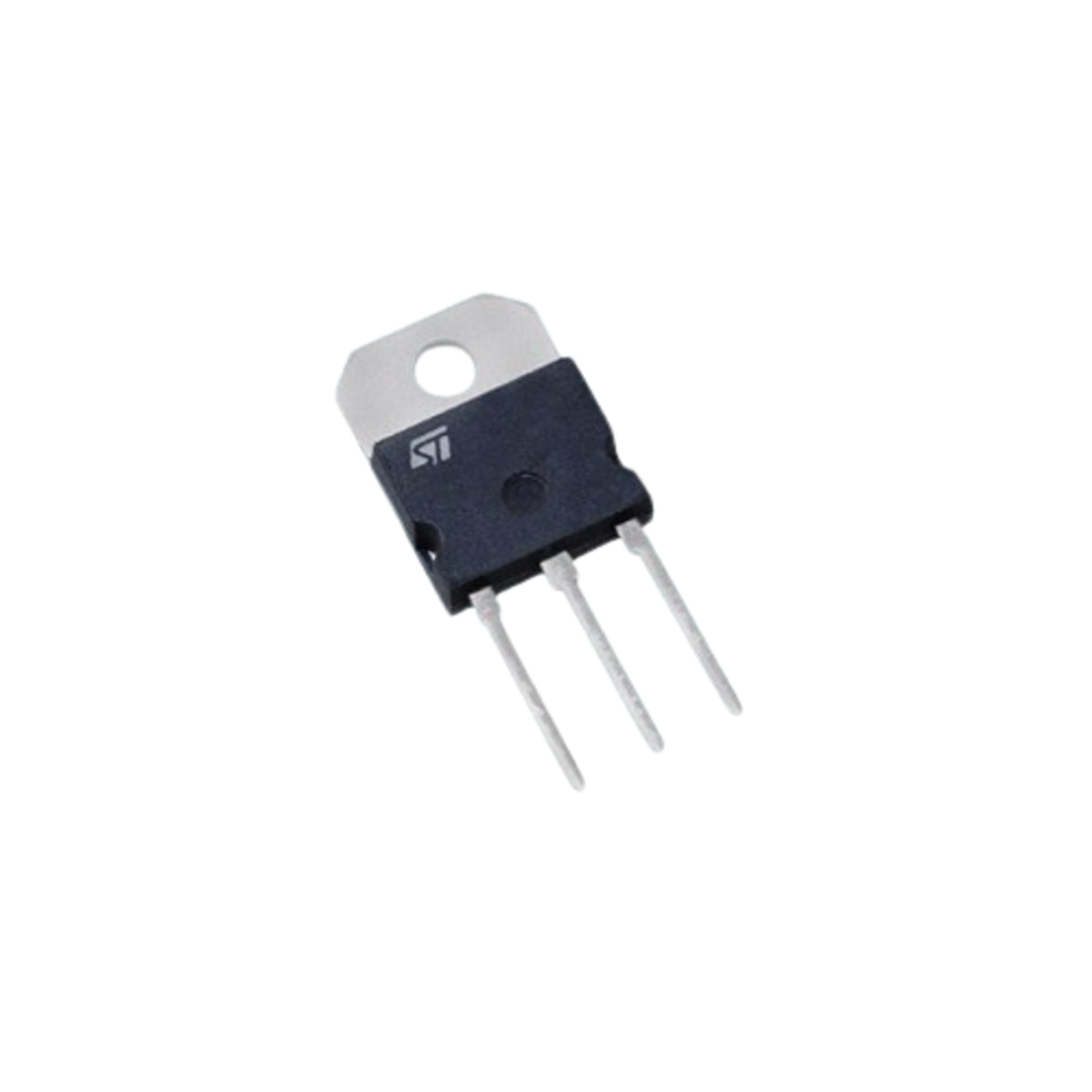 BDW83C NPN Darlington Power Transistor (15A, 150W, TO 3P, 1 Qty)
TRD-74
₹ 53.10 (Incl. GST)
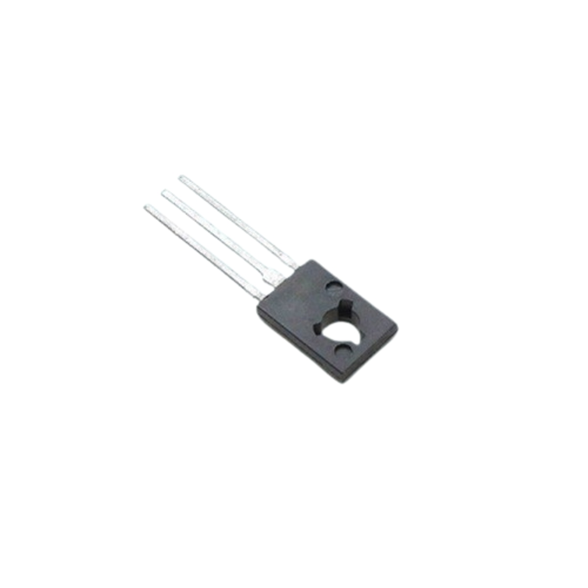 BD681 NPN Darlington Power Transistor (100V, 4A, TO 126, 1 Qty)
TRD-68
₹ 17.70 (Incl. GST)
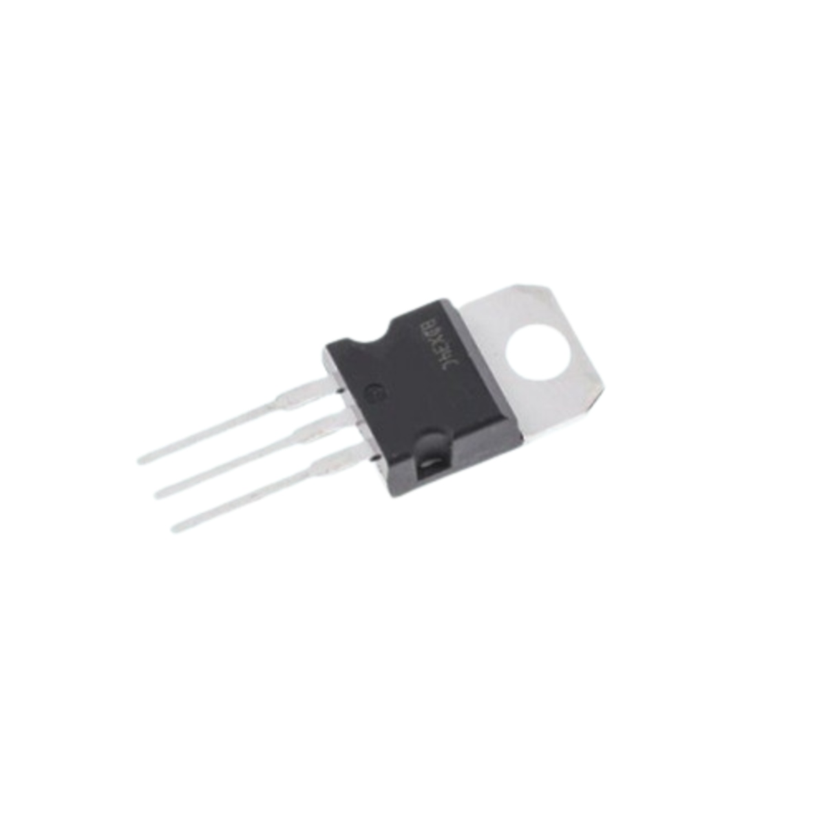 BDX34C PNP Darlington Power Transistor (100V, 10A, TO 220, 1 Qty)
TRD-69
₹ 53.10 (Incl. GST)
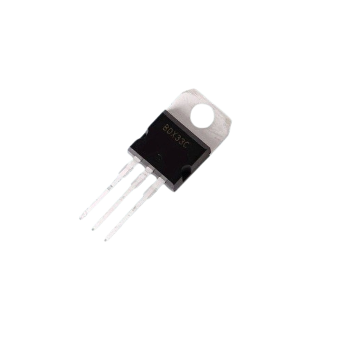 BDX33C NPN Darlington Power Transistor (100V, 10A, TO 220, 1 Qty)
TRD-70
₹ 23.60 (Incl. GST)
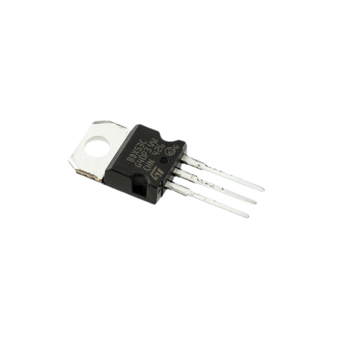 BDX53C NPN Darlington Power Transistor (100V, 8A, 60W, TO 220, 1 Qty)
TRD-71
₹ 23.60 (Incl. GST)
 BDW84C Darlington Power PNP Transistor TO-3P (BDW84C Power Transistor)
TRD-72
₹ 53.10 (Incl. GST)
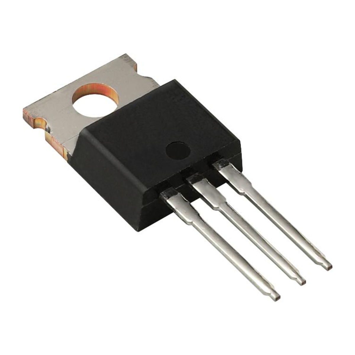 BDX34B PNP Darlington Power Transistor (80V, 10A, 70W, TO 220, 1 Qty)
TRD-73
₹ 53.10 (Incl. GST)
 BU807 NPN Darlington Power Transistor (TO 220, 1 Qty)
TRD-77
₹ 27.10 (Incl. GST)
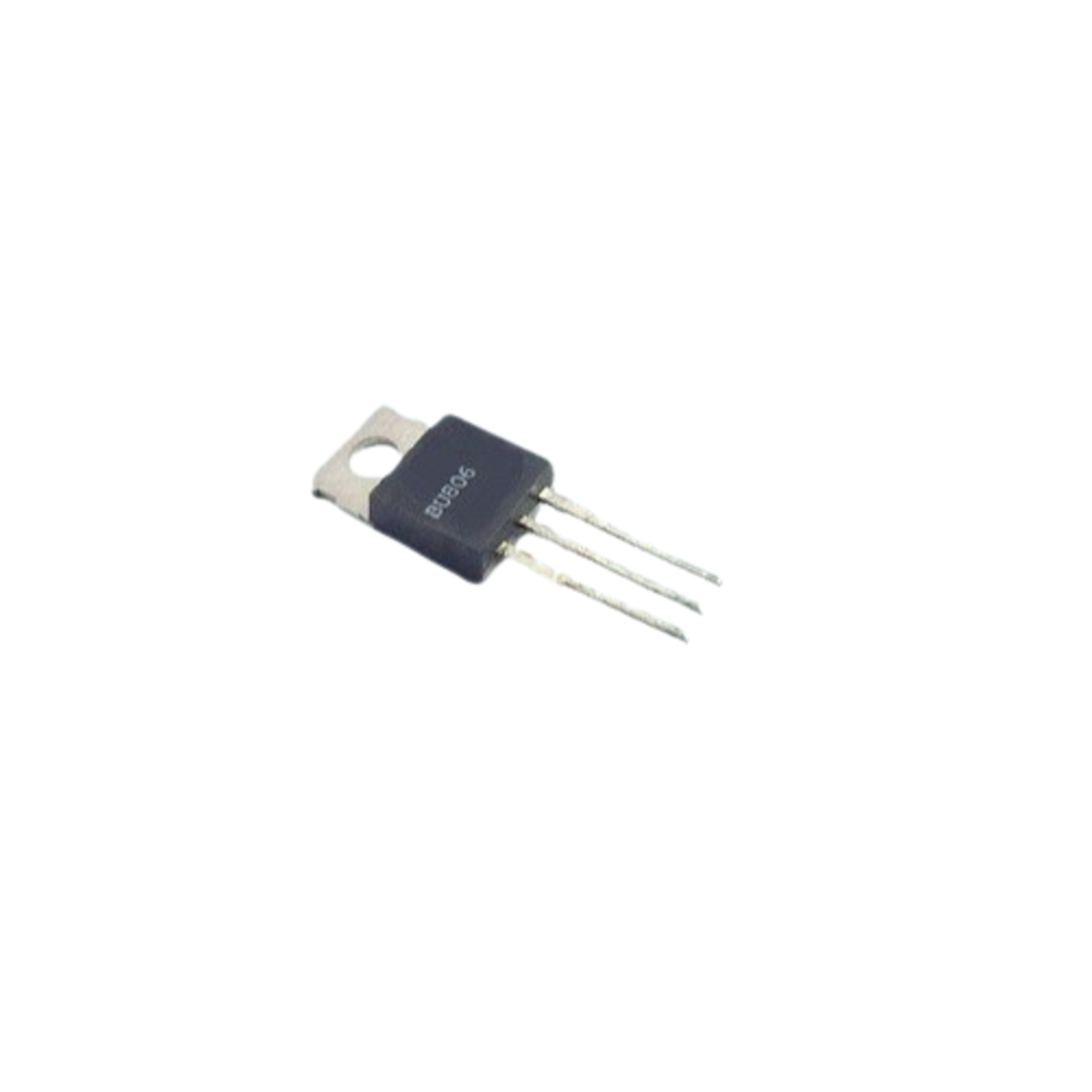 BU806 Multicomp Pro NPN Darlington Power Transistor (200V, 8A, 60W, TO 220, 1 Qty)
TRD-80
₹ 35.40 (Incl. GST)
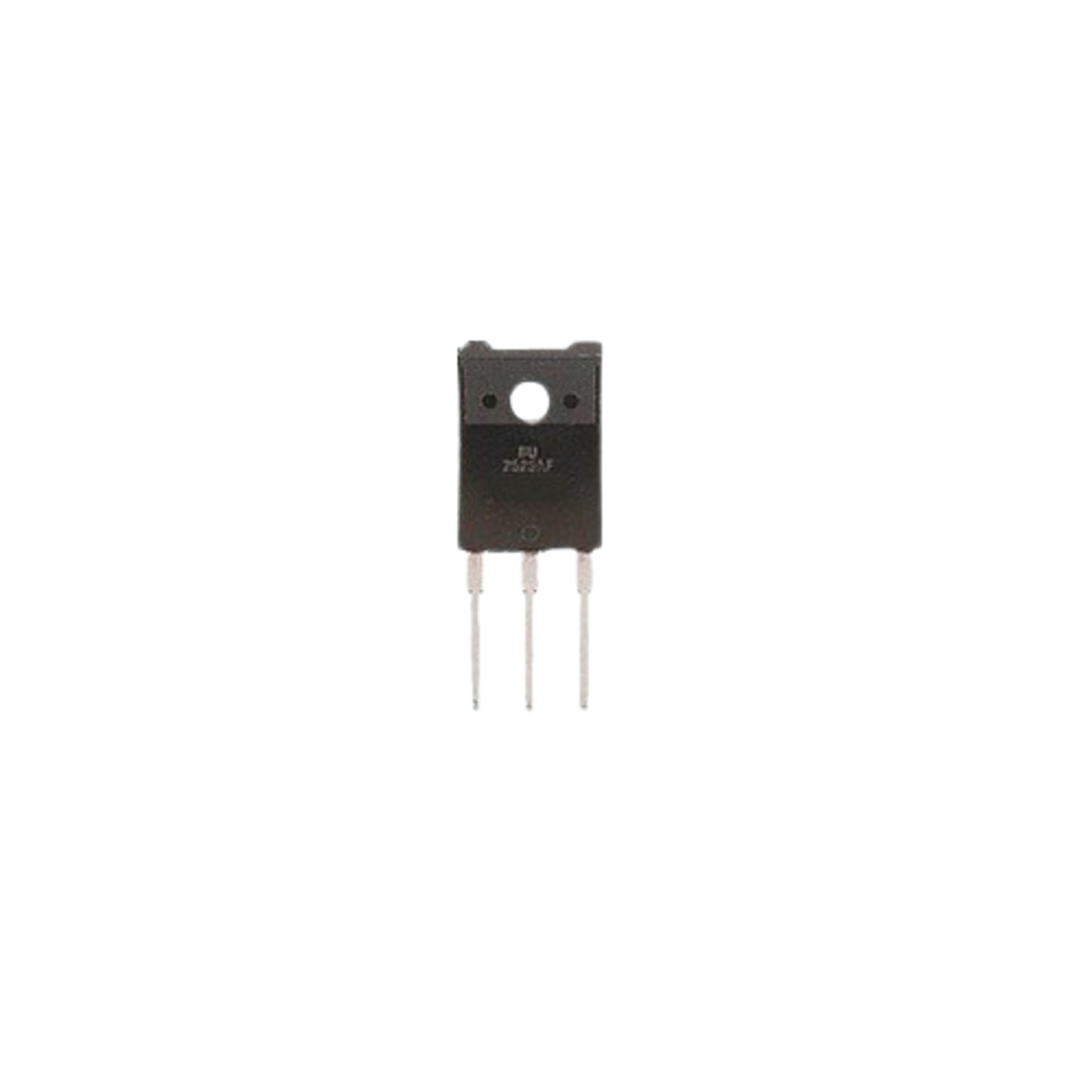 BU2508AF Silicon NPN Power Transistor (1500V, 8A, 80W, TO 247, 1 Qty)
TRD-79
₹ 118.00 (Incl. GST)