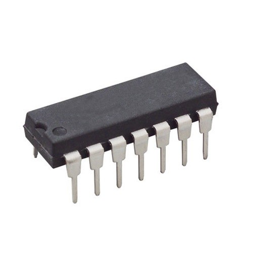
MC145436P Dual Tone Multiple Frequency (DTMF) Receiver DIP-14 (MC145436P DIP IC)
The MC145436P is a high-performance monolithic silicon-gate CMOS integrated circuit designed for DTMF (Dual Tone Multiple Frequency) detection. It integrates the necessary bandsplit filters and digital decoding functions to detect and decode all 16 standard DTMF tone pairs. This IC features a built-in switched-capacitor filter for high and low group separation, followed by a digital frequency detection stage that ensures high immunity to "talk-off" (false triggering by speech or noise). The decoded output is provided in a 4-bit binary format, making it easy to interface with microcontrollers.
This IC is primarily used in telephone answering machines, remote control systems over phone lines, and credit card verification terminals. It is a vital component for Arduino electronics projects in India involving DTMF-controlled robotics, remote home automation via mobile calls, and IVR (Interactive Voice Response) system prototypes.
Key Features
- Complete DTMF receiver on a single chip
- Low power consumption (CMOS technology)
- Excellent noise immunity and "talk-off" performance
- Internal switched-capacitor bandsplit filters
- Decodes all 16 standard DTMF digits (0-9, A-D, *, #)
- 4-bit binary (BCD) output with data valid flag
- Internal clock generator (requires 3.579MHz crystal)
- Wide supply voltage range (4.5V to 5.5V)
Specifications
- IC Type = DTMF Receiver / Decoder
- Logic Family = CMOS
- Supply Voltage = 4.5V to 5.5V (5V Typical)
- Operating Current = 7mA (Maximum)
- Clock Frequency = 3.579545 MHz (External Crystal)
- Output Format = 4-Bit Binary (BCD)
- Package Type = DIP
- Number of Pins = 14
- Mounting Type = Through-Hole
- Operating Temperature = -40 to 85 degrees Celsius
Interfaces
- PIN 1 (IN+) = Non-Inverting Op-Amp Input
- PIN 2 (IN-) = Inverting Op-Amp Input
- PIN 3 (GS) = Gain Select Output (Op-Amp Output)
- PIN 4 (VREF) = Reference Voltage Output
- PIN 5 (VSS) = Ground (0V)
- PIN 6 (OSC1) = Crystal Oscillator Input
- PIN 7 (OSC2) = Crystal Oscillator Output
- PIN 8 (DV) = Data Valid Output (Active High)
- PIN 9 to 12 (Q1, Q2, Q3, Q4) = 4-Bit Binary Data Outputs
- PIN 13 (TOE) = Three-State Output Enable
- PIN 14 (VDD) = Positive Supply Voltage (5V)