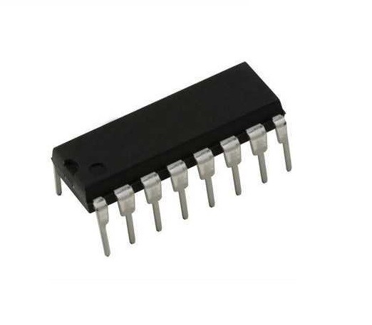
MC145503P Pulse Code Modulation (PCM) Codec-Filter DIP-20 (MC145503P DIP IC) The MC145503P is a high-performance monolithic PCM Codec-Filter (Coder-Decoder) designed for digital telephone systems. It combines a voice-band bandpass filter and an analog-to-digital converter (Encoder) with a digital-to-analog converter (Decoder) and a low-pass reconstruction filter on a single chip. This IC utilizes Mu-Law companding, which is the standard for digital voice compression in North American and Japanese telecommunication networks. It is engineered to provide high-quality voice transmission while minimizing data bandwidth requirements.
This IC is primarily used in digital private branch exchange (PBX) systems, digital telephone sets, and voice-over-IP (VoIP) hardware. It is a specialized component for advanced Arduino electronics projects in India involving digital voice recording, custom telecommunication interface design, or building DIY digital intercom systems using standard PCM data formats.
Key Features
- Complete PCM Codec and Filter system on one chip
- Mu-Law companding for high-quality voice compression
- Precision internal voltage reference for stable operation
- Integrated bandpass transmit filter and low-pass receive filter
- Low power consumption (typically 30mW)
- Power-down mode for energy efficiency (0.5mW)
- Synchronous or asynchronous operation capability
- TTL and CMOS compatible digital interface
Specifications
- IC Type = PCM Codec-Filter (Mu-Law)
- Supply Voltage = 4.75V to 5.25V (5V Typical)
- Logic Family = CMOS / TTL Compatible
- Data Format = 8-Bit Serial PCM
- Companding Standard = Mu-Law
- Package Type = Plastic DIP
- Number of Pins = 20
- Mounting Type = Through-Hole
- Operating Temperature = -40 to 85 degrees Celsius
Interfaces
- PIN 1 (VDD) = Positive Power Supply (5V)
- PIN 2 (VSS) = Negative Power Supply or Ground (0V)
- PIN 3 (VAG) = Analog Ground Reference
- PIN 4 (ROUT+) = Non-Inverting Analog Receive Output
- PIN 5 (ROUT-) = Inverting Analog Receive Output
- PIN 6 (FSR) = Frame Sync Receive Input
- PIN 7 (BCLKR) = Bit Clock Receive Input
- PIN 8 (DR) = Digital Receive Data Input
- PIN 11 (DT) = Digital Transmit Data Output
- PIN 12 (BCLKT) = Bit Clock Transmit Input
- PIN 13 (FST) = Frame Sync Transmit Input
- PIN 18 (AIN+) = Non-Inverting Analog Transmit Input
- PIN 19 (AIN-) = Inverting Analog Transmit Input