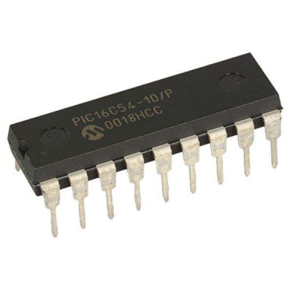
PIC16F54-I/SP 8-Bit Flash Microcontroller Baseline Core DIP-18 (PIC16F54-I/SP DIP IC)
The PIC16F54-I/SP is an entry-level, 8-bit Flash-based microcontroller belonging to Microchip’s "Baseline" family. Housed in an 18-pin Skinny DIP package, it is designed for simple, high-volume applications where low cost and small code footprints are the primary requirements. It features a simplified RISC architecture with only 33 single-word instructions. This IC includes 768 bytes of Flash program memory and 25 bytes of RAM. While it lacks some of the integrated analog peripherals found in the mid-range series, its high speed, low power consumption, and wide operating voltage make it a reliable and robust choice for basic logic replacement and timing tasks.
This IC is primarily used in consumer appliances, electronic toys, and basic lighting controllers. It is a common component for Arduino electronics projects in India for building DIY logic gates, simple LED flasher circuits, and educational projects where students learn the fundamentals of RISC assembly and low-level hardware control in a standard 18-pin DIP footprint.
Key Features
- Baseline RISC CPU with 33 single-word instructions
- High-speed execution (200ns instruction cycle at 20MHz)
- 12 bidirectional I/O pins with individual direction control
- Power-on Reset (POR) and Device Reset Timer (DRT)
- Watchdog Timer (WDT) with its own on-chip RC oscillator for reliability
- Low-power consumption (under 2mA at 5V, 4MHz)
- Wide operating voltage range (2.0V to 6.25V)
- In-Circuit Serial Programming (ICSP) support
- Programmable code protection for firmware security
- High current source/sink for direct LED drive
Specifications
- IC Type = 8-Bit Flash Microcontroller
- Program Memory = 768 Bytes (512 Words)
- Data RAM = 25 bytes
- Maximum Speed = 20MHz (External)
- I/O Pins = 12 (Ports A and B)
- Supply Voltage = 2.0V to 6.25V
- Current Sink/Source = 25mA
- Package Type = SPDIP-18 (Skinny DIP)
- Number of Pins = 18
- Mounting Type = Through-Hole
- Operating Temperature = -40 to 85 degrees Celsius
Interfaces
- PIN 1 (RA2) = Port A I/O
- PIN 2 (RA3) = Port A I/O
- PIN 3 (T0CKI) = Timer 0 Clock Input
- PIN 4 (MCLR) = Master Clear / Reset Input
- PIN 5 (VSS) = Ground (0V)
- PIN 6 to 13 (RB0 to RB7) = 8-Bit Port B I/O / ICSP Data and Clock
- PIN 14 (VDD) = Positive Supply Voltage (5V)
- PIN 15 (OSC2/CLKOUT) = Oscillator Output
- PIN 16 (OSC1/CLKIN) = Oscillator Input
- PIN 17 (RA0) = Port A I/O
- PIN 18 (RA1) = Port A I/O