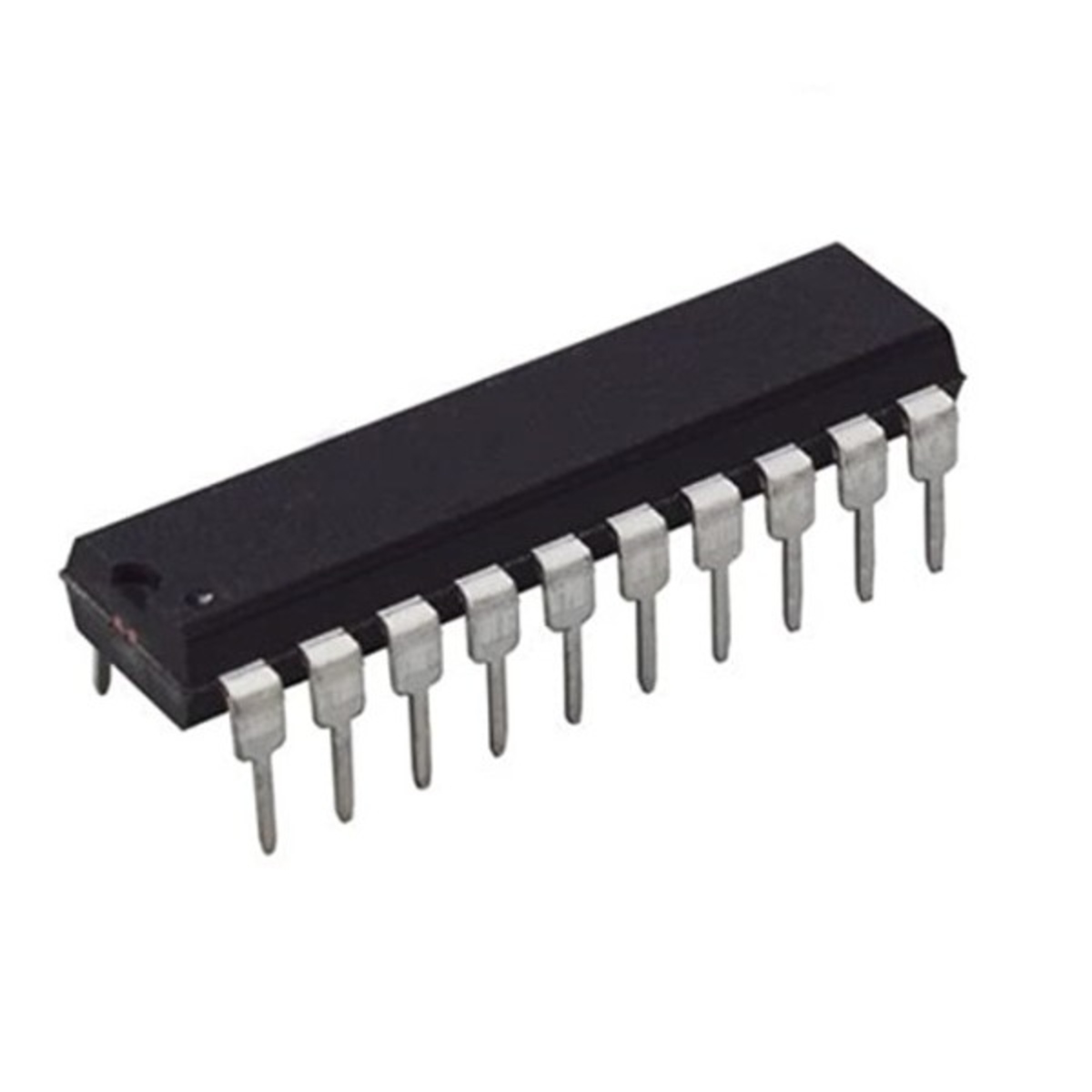
74LS377 DIP-20 Octal D-Type Flip-Flop IC (Common Enable, TTL, 5V)
Description -
The 74LS377 DIP is a TTL logic integrated circuit that functions as an octal D-type flip-flop in a 20-pin Dual Inline Package (DIP). It belongs to the 74LS Low Power Schottky logic family and is designed for parallel data storage, data buffering, and register applications in synchronous digital systems.
The device contains eight D-type flip-flops with a common clock and common enable input, allowing all eight bits of data to be stored simultaneously on the rising edge of the clock when enabled. The 74LS377 is widely used in microprocessor systems, digital registers, embedded systems, and data storage applications.
Key Features -
• Octal D-type flip-flops
• Common clock and enable inputs
• Positive edge-triggered operation
• Parallel data input and output
• Low Power Schottky technology
• TTL compatible logic levels
• High-speed switching performance
• Standard DIP-20 package
Specifications -
• Product type - TTL Logic IC
• IC Model - 74LS377
• Logic Function - Octal D-Type Flip-Flop
• Package type - DIP-20
• Logic family - 74LS TTL
• Operating voltage - 4.75V to 5.25V DC
• Number of flip-flops - 8
• Trigger type - Positive Edge
• Control inputs - Common Clock and Enable
• Output type - Standard TTL
• Operating temperature - 0C to 70C
Applications -
• Data registers
• Data buffering
• Parallel data storage
• Microprocessor systems
• Embedded systems
• Digital control circuits
• Industrial automation
• Sequential logic applications