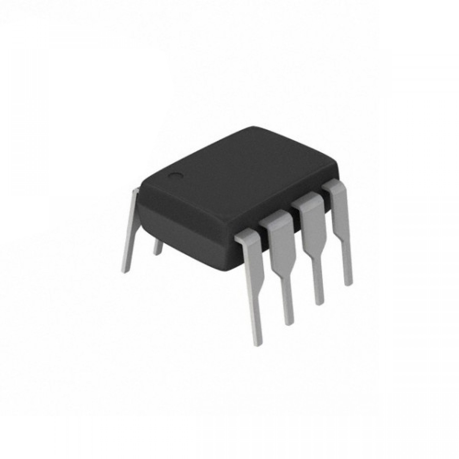
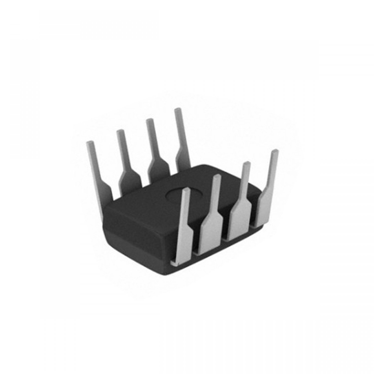
DS1210 Nonvolatile Controller Chip DIP-8 (DS1210 IC)
The DS1210 is a specialized CMOS nonvolatile controller IC designed to convert standard static CMOS RAM into nonvolatile memory. Housed in a compact 8-pin DIP package, it provides a seamless solution for preserving data in the event of a power failure. The IC continuously monitors incoming power (VCCI); when it detects an out-of-tolerance condition, it automatically write-protects the RAM by inhibiting the Chip Enable (CE) signal and switches to battery backup to ensure uninterrupted power to the memory. Its low-leakage CMOS process ensures extremely low battery consumption, typically drawing less than 100nA, making it an industry standard for data retention applications.
This IC is primarily used in industrial controllers, point-of-sale terminals, and embedded systems where critical data like system settings or transaction logs must be preserved without power. It is a popular component for electronics projects in India for building DIY battery-backed RAM modules, vintage computer restorations, and smart data loggers that require reliable nonvolatile storage without the write-cycle limitations of EEPROM or Flash.
Key Features
- Converts standard CMOS SRAM into Nonvolatile Memory
- Unconditional write protection when VCC is out of tolerance
- Automatic battery switching during power-fail events
- Redundant battery support with internal isolation switching
- Extremely low battery current consumption (typically <100nA)
- Automatic battery condition testing on power-up
- Dual-range power-fail detection (5% or 10% tolerance)
- Low forward voltage drop on the power switch (typically <0.3V)
- Precision comparator for accurate voltage monitoring
- Minimal propagation delay (max 20ns) for Chip Enable signal
Specifications
- IC Type = Nonvolatile RAM Controller
- Supply Voltage (VCCI) = 4.5V to 5.5V
- Battery Input Voltage = 2.0V to 4.0V
- Operating Supply Current = 5mA (Max)
- Battery Backup Current = 100nA (Typical)
- RAM Output Current (ICCO1) = 80mA (Max)
- Trip Point (TOL=GND) = 4.5V to 4.74V (10% Tolerance)
- Trip Point (TOL=VCCO) = 4.25V to 4.49V (5% Tolerance)
- CE to CEO Delay = 20ns (Max)
- Package Type = PDIP-8
- Number of Pins = 8
- Mounting Type = Through-Hole
- Operating Temperature = 0 to 70 degrees Celsius
Interfaces
- PIN 1 (VCCO) = RAM Supply Output (switches between VCCI and Battery)
- PIN 2 (VBAT1) = + Connection for Primary Battery
- PIN 3 (TOL) = Power Supply Tolerance Select (GND for 10%, VCCO for 5%)
- PIN 4 (GND) = Ground (0V)
- PIN 5 (CE) = Chip Enable Input from Microprocessor
- PIN 6 (CEO) = Chip Enable Output to RAM (inhibited during power-fail)
- PIN 7 (VBAT2) = + Connection for Redundant Battery (ground if not used)
- PIN 8 (VCCI) = + Supply Input (main system power)