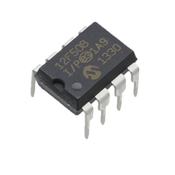
PIC12F508-I/P 8-Bit Flash Microcontroller DIP-8 (PIC12F508 I/P DIP IC)
The PIC12F508-I/P is a low-cost, high-performance 8-bit Flash-based microcontroller. It utilizes a high-performance RISC CPU with only 33 single-word instructions. This IC includes 512 words of Flash program memory and 25 bytes of RAM. Unlike the older "C" series, the "F" series features Electrically Erasable Flash memory, allowing the chip to be reprogrammed multiple times. It features an internal 4MHz RC oscillator and a very small 8-pin footprint, making it an ideal solution for applications where cost, space, and low power consumption are primary requirements.
This IC is primarily used in low-power remote transmitters, security systems, and simple appliance controllers. It is a fundamental component for Arduino electronics projects in India involving standalone logic control, building customized interval timers, and learning PIC assembly or C programming on a compact 8-pin platform.
Key Features
- High-performance RISC CPU with 33 instructions
- Reprogrammable Flash memory (re-writable)
- Internal 4MHz RC oscillator with programmable calibration
- In-Circuit Serial Programming (ICSP) support
- Wide operating voltage range (2.0V to 5.5V)
- Extremely low power consumption (under 2uA standby at 2V)
- 8-bit real-time clock/counter (TMR0) with 8-bit programmable prescaler
- Watchdog Timer (WDT) with independent on-chip RC oscillator
- High current source/sink for direct LED drive (25mA)
Specifications
- IC Type = 8-Bit Flash Microcontroller
- Program Memory = 512 Words (768 Bytes)
- Data RAM = 25 Bytes
- Speed = 4MHz (Internal Oscillator)
- I/O Pins = 6 (5 I/O, 1 Input-only)
- Supply Voltage = 2.0V to 5.5V
- Current Sink/Source = 25mA
- Package Type = PDIP-8
- Number of Pins = 8
- Mounting Type = Through-Hole
- Operating Temperature = -40 to 85 degrees Celsius
Interfaces
- PIN 1 (VDD) = Positive Supply Voltage (5V)
- PIN 2 (GP5/OSC1/CLKIN) = General Purpose I/O / Oscillator Input
- PIN 3 (GP4/OSC2/CLKOUT) = General Purpose I/O / Oscillator Output
- PIN 4 (GP3/MCLR/VPP) = Input Only / Master Clear / Programming Voltage
- PIN 5 (GP2/T0CKI) = General Purpose I/O / Timer Clock Input
- PIN 6 (GP1/ICSPCLK) = General Purpose I/O / Programming Clock
- PIN 7 (GP0/ICSPDAT) = General Purpose I/O / Programming Data
- PIN 8 (VSS) = Ground (0V)